Report an Error

NVIDIA GM20B
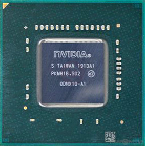
ODNX10-A1
NVIDIA's GM20B GPU uses the Maxwell 2.0 architecture and is made using a 16 nm production process at TSMC. With a die size of 100 mm² and a transistor count of 2,000 million it is a small chip. GM20B supports DirectX 12 (Feature Level 12_1). For GPU compute applications, OpenCL version 1.2 and CUDA 5.3 can be used. It features 256 shading units, 16 texture mapping units and 16 ROPs.
Further reading:
Tegra X1 Architecture Whitepaper 
Graphics Processor
- Released
- Aug 16th, 2019
- GPU Name
- GM20B
- Codename
- NV12B
- Architecture
- Maxwell 2.0
- Foundry
- TSMC
- Process Size
- 16 nm
- Transistors
- 2,000 million
- Density
- 20.0M / mm²
- Die Size
- 100 mm²
Graphics Features
- DirectX
- 12 (12_1)
- OpenGL
- 4.6
- OpenCL
- 1.2
- Vulkan
- 1.1
- CUDA
- 5.3
- Shader Model
- 6.0
- PureVideo HD
- VP9
- VDPAU
- Feature Set I
Render Config
- Shading Units
- 256
- TMUs
- 16
- ROPs
- 16
- SMM Count
- 2
- Max. TDP
- 15 W
- GPCs
- 1
- SFUs
- 128
All Maxwell 2.0 GPUs
- NVIDIA GM200
- NVIDIA GM204
- NVIDIA GM206
- NVIDIA GM206S
- NVIDIA GM20B
- NVIDIA GM20B
NVIDIA GPU Architecture History
- 2024 Blackwell
- 2023 Hopper
- 2022-2024 Ada Lovelace
- 2020-2024 Ampere
- 2018-2022 Turing
- 2017-2020 Volta
- 2016-2021 Pascal
- 2014-2019 Maxwell 2.0
- 2014-2017 Maxwell
- 2013-2015 Kepler 2.0
- 2012-2018 Kepler
- 2010-2016 Fermi 2.0
- 2010-2013 VLIW Vec4
- 2010-2016 Fermi
- 2007-2013 Tesla 2.0
- 2006-2010 Tesla
- 2003-2013 Curie
- 2003-2005 Rankine
- 2001-2003 Kelvin
- 1999-2005 Celsius
- 1998-2000 Fahrenheit
Graphics cards using the NVIDIA GM20B GPU
| Name | Chip | Memory | Shaders | TMUs | ROPs | Base Clock | Boost Clock | Memory Clock |
|---|---|---|---|---|---|---|---|---|
| ODNX10-A1 | 4 GB | 256 | 16 | 16 | 384 MHz | 768 MHz | 1600 MHz |

GM20B GPU Notes
| PureVideo HD: VP9 VDPAU: Feature Set I |
Jun 1st, 2024 18:55 EDT
change timezone
Latest GPU Drivers
New Forum Posts
- What are you playing? (20775)
- SSD cooling advice (4)
- V Rising Lycanthropy Club (9)
- How to reduce Asus mining rx470 4096 mb to 2048 mb vram? (4)
- Your PC ATM (34594)
- Core counting (67)
- Dude, youre hotrodding a Dell... (0)
- Would you pay more for hardware with AI capabilities? (87)
- 3D/Game Design Workstation (7)
- What's your latest tech purchase? (20716)
Popular Reviews
- ID-Cooling FX360 PRO Review - Shots Fired @ Arctic
- SilverStone KL07E Review
- NuPhy Air96 V2 Low Profile Wireless Mechanical Keyboard Review
- Senua’s Saga: Hellblade II: DLSS vs. FSR vs. XeSS Comparison Review
- Upcoming Hardware Launches 2024 (Updated May 2024)
- Montech Titan Gold 1000 W Review
- Elysian Acoustic Labs Pilgrim In-Ear Monitors Review
- Waizowl OGM Cloud Review
- Ghost of Tsushima Performance Benchmark Review - 35 GPUs Tested
- Senua's Saga: Hellblade II Performance Benchmark Review
Controversial News Posts
- AMD to Redesign Ray Tracing Hardware on RDNA 4 (227)
- NVIDIA to Only Launch the Flagship GeForce RTX 5090 in 2024, Rest of the Series in 2025 (154)
- AMD Hits Highest-Ever x86 CPU Market Share in Q1 2024 Across Desktop and Server (140)
- AMD RDNA 5 a "Clean Sheet" Graphics Architecture, RDNA 4 Merely Corrects a Bug Over RDNA 3 (139)
- NVIDIA RTX 5090 "Blackwell" Founders Edition to Implement the "RTX 4090 Ti" Cinderblock Design (116)
- Core Configurations of Intel Core Ultra 200 "Arrow Lake-S" Desktop Processors Surface (101)
- Biden Administration to Revive Trump-Era Tariffs on China-made GPUs and Motherboards (95)
- AMD Ryzen 9000 Zen 5 Single Thread Performance at 5.80 GHz Found 19% Over Zen 4 (87)