 45
45
MSI GeForce RTX 4090 Gaming X Trio Review
(45 Comments) »Introduction
NVIDIA GeForce RTX 4090 is the green team's flagship card based on the Ada GPU architecture. The card was released in October 2022 and has established itself as "the best, at a price." During our original launch day coverage I reviewed eight (!) GeForce RTX 4090 cards, today we're checking out the ninth one. Last year I've tested the MSI RTX 4090 Suprim X and the RTX 4090 Suprim X Liquid. In today's review I'll look at the MSI GeForce RTX 4090 Gaming X Trio, which is the company's most affordable RTX 4090 card available.
Actually, based on the listings at Newegg, it's the most affordable RTX 4090 card available overall, at $1700, which is why I asked MSI for a chance to run this card through our extensive tests to determine whether this RTX 4090 is able to compete with the more expensive offerings available, which go up $2600—almost $1000 more.
With this review we're also introducing our brand-new GPU 2023.1 test suite, which uses a Core i9-13900K, paired with the EVGA Z790 DARK, 32 GB of fast DDR5 memory, Seasonic's newest ATX 3.0 power supply and Windows 11. We also added several new games for both ray tracing and rasterization, and there's now an expanded minimum FPS section showing the results for all games we've tested, plus two new summary charts for minimum FPS.

The GeForce RTX 4090 is NVIDIA's top dog, built using the mammoth AD102 graphics processor, which comes with 76.3 billion transistors, 16,384 GPU cores, 24 GB GDDR6X over a 384-bit wide bus and support for all the newest technologies like DLSS 3 Frame Generation, improved tensor cores, faster ray tracing and shader-execution reordering.
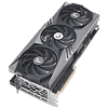
MSI's GeForce RTX 4090 Gaming X Trio that we test in this review is a custom-design implementation with a large triple-slot, triple-fan cooling solution. The VRM design is a powerful 18+4 configuration with the Monolithic MP2891 controller. At the same time the card is carefully designed to not break, yet offer the same fantastic experience that other, more expensive RTX 4090 cards deliver. In terms of factory overclocks you're getting an increase of 75 MHz GPU frequency over the NVIDIA Founders Edition, or 3%. As mentioned before, while MSI is pricing their card competitively against other offerings, there's still a $100 increase over the $1,600 NVIDIA RTX 4090 MSRP.
| Price | Cores | ROPs | Core Clock | Boost Clock | Memory Clock | GPU | Transistors | Memory | |
|---|---|---|---|---|---|---|---|---|---|
| RTX 3070 | $400 | 5888 | 96 | 1500 MHz | 1725 MHz | 1750 MHz | GA104 | 17400M | 8 GB, GDDR6, 256-bit |
| RTX 3070 Ti | $520 | 6144 | 96 | 1575 MHz | 1770 MHz | 1188 MHz | GA104 | 17400M | 8 GB, GDDR6X, 256-bit |
| RX 6800 | $480 | 3840 | 96 | 1815 MHz | 2105 MHz | 2000 MHz | Navi 21 | 26800M | 16 GB, GDDR6, 256-bit |
| RX 6800 XT | $560 | 4608 | 128 | 2015 MHz | 2250 MHz | 2000 MHz | Navi 21 | 26800M | 16 GB, GDDR6, 256-bit |
| RTX 3080 | $570 | 8704 | 96 | 1440 MHz | 1710 MHz | 1188 MHz | GA102 | 28000M | 10 GB, GDDR6X, 320-bit |
| RTX 3080 Ti | $750 | 10240 | 112 | 1365 MHz | 1665 MHz | 1188 MHz | GA102 | 28000M | 12 GB, GDDR6X, 384-bit |
| RX 6900 XT | $680 | 5120 | 128 | 2015 MHz | 2250 MHz | 2000 MHz | Navi 21 | 26800M | 16 GB, GDDR6, 256-bit |
| RX 6950 XT | $800 | 5120 | 128 | 2100 MHz | 2310 MHz | 2250 MHz | Navi 21 | 26800M | 16 GB, GDDR6, 256-bit |
| RTX 3090 | $850 | 10496 | 112 | 1395 MHz | 1695 MHz | 1219 MHz | GA102 | 28000M | 24 GB, GDDR6X, 384-bit |
| RTX 4070 Ti | $820 | 7680 | 80 | 2310 MHz | 2610 MHz | 1313 MHz | AD104 | 35800M | 12 GB, GDDR6X, 192-bit |
| RX 7900 XT | $880 | 5376 | 192 | 2000 MHz | 2400 MHz | 2500 MHz | Navi 31 | 57700M | 20 GB, GDDR6, 320-bit |
| RTX 3090 Ti | $1400 | 10752 | 112 | 1560 MHz | 1950 MHz | 1313 MHz | GA102 | 28000M | 24 GB, GDDR6X, 384-bit |
| RTX 4080 | $1200 | 9728 | 112 | 2205 MHz | 2505 MHz | 1400 MHz | AD103 | 45900M | 16 GB, GDDR6X, 256-bit |
| RX 7900 XTX | $1000 | 6144 | 192 | 2300 MHz | 2500 MHz | 2500 MHz | Navi 31 | 57700M | 24 GB, GDDR6, 384-bit |
| RTX 4090 | $1600 | 16384 | 176 | 2235 MHz | 2520 MHz | 1313 MHz | AD102 | 76300M | 24 GB, GDDR6X, 384-bit |
| MSI RTX 4090 Gaming X Trio | $1700 | 16384 | 176 | 2235 MHz | 2595 MHz | 1313 MHz | AD102 | 76300M | 24 GB, GDDR6X, 384-bit |
Packaging


The Card


The MSI Gaming X is dominated by black, with various shades of gray as highlights. On the rear you'll find a high-quality metal backplate.

MSI has integrated two RGB illuminated elements in the front cooler and one along the top edge of the card.


Dimensions of the card are 34.0 x 14.0 cm, and it weighs 2195 g.


Installation requires three slots in your system.

Display connectivity includes three standard DisplayPort 1.4a ports and one HDMI 2.1a (same as Ampere).
NVIDIA introduced the concept of dual NVDEC and NVENC Codecs with the Ada architecture. This means there are two independent sets of hardware-accelerators; so you can encode and decode two streams of video in parallel or one stream at double the FPS rate. The new 8th Gen NVENC now accelerates AV1 encoding, besides HEVC. You also get an "optical flow accelerator" unit that is able to calculate intermediate frames for videos, to smooth playback. The same hardware unit is used for frame generation in DLSS 3.

The card uses the new 12+4 pin ATX 12VHPWR connector, which is rated for up to 600 W of power draw. An adapter cable from 4x PCIe 8-pin is included, you can also run the card with just three 8-pins.

This BIOS switch lets you toggle from the default quiet BIOS to the gaming BIOS, which runs a more aggressive fan curve.
Teardown


MSI'S thermal solution is big and powerful. While the Suprim X has a vapor-chamber, the Gaming X Trio has a classic baseplate, which soaks up heat from the GPU quickly and moves it through eight heatpipes to the heatsink. The main heatsink also provides cooling for the VRM and memory chips.


Once the main cooler assembly is removed, a metal frame is revealed, which helps protect against bending and sagging.
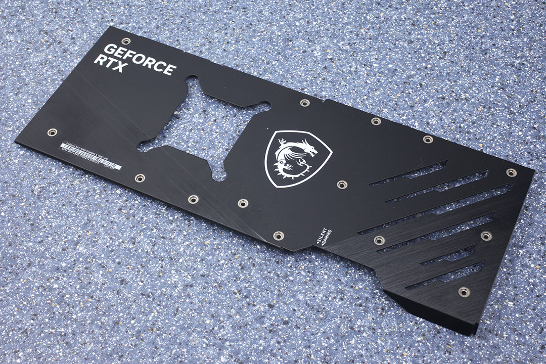

The backplate is made from thick metal and is of excellent build quality. It protects the card against damage during installation and handling. Note the thermal pads and the cable for the RGB element.
High-resolution PCB Pictures
These pictures are for the convenience of volt modders and people who would like to see all the finer details on the PCB. Feel free to link back to us and use these in your articles, videos or forum posts.

High-resolution versions are also available (front, back).
Circuit Board (PCB) Analysis


GPU voltage is a massive 18-phase design managed by a Monolithic Power Systems MP2891 controller, which also handles memory voltage.

OnSemi NCP303151A DrMOS components are used for GPU voltage; they are rated for 50 A of current each.

Memory voltage is a four-phase design, managed by the same MP2891 that's uses for GPU voltage.

For memory, OnSemi NCP303151A DrMOS with a 50 A rating are used too.
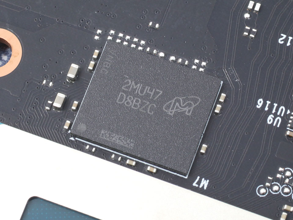
The GDDR6X memory chips are made by Micron and carry the model number D8BZC, which decodes to MT61K512M32KPA-21:U. They are specified to run at 1313 MHz (21 Gbps effective).

NVIDIA's AD102 graphics processor is the company's flagship Ada Lovelace GPU. It's the world's first 5 nanometer GPU, built at TSMC Taiwan with a transistor count of 76.3 billion and a die size of 608 mm².
Our Patreon Silver Supporters can read articles in single-page format.
May 18th, 2024 08:02 EDT
change timezone
Latest GPU Drivers
New Forum Posts
- Page load time extension results for popular websites (14)
- What are you playing? (20674)
- Ghost of Tsushima PC Port !!!! (55)
- is there anyway to verify my motherboard actually has a gen5 gpu slot without a gen5 card? (24)
- PSU Option for my PC (18)
- EK seems to be having major issues (98)
- Cannot locate ASRock rx6800 Challenger pro OC VBIOS update (1)
- AIO Water Cooler vs Tower Air Cooler (48)
- Would you pay more for hardware with AI capabilities? (32)
- What's your latest tech purchase? (20559)
Popular Reviews
- Ghost of Tsushima Performance Benchmark Review - 35 GPUs Tested
- Homeworld 3 Performance Benchmark Review - 35 GPUs Tested
- Lofree Edge Ultra-Low Profile Wireless Mechanical Keyboard Review
- Silverstone Shark Force 120 mm Fan Review
- Enermax REVOLUTION D.F. X 1200 W Review
- Sapphire Radeon RX 7900 GRE Pulse Review
- Upcoming Hardware Launches 2023 (Updated Feb 2024)
- TerraMaster D8 Hybrid Review
- AMD Ryzen 7 7800X3D Review - The Best Gaming CPU
- ZMF Caldera Closed Planar Magnetic Headphones Review
Controversial News Posts
- Intel Statement on Stability Issues: "Motherboard Makers to Blame" (269)
- AMD to Redesign Ray Tracing Hardware on RDNA 4 (227)
- Windows 11 Now Officially Adware as Microsoft Embeds Ads in the Start Menu (172)
- NVIDIA to Only Launch the Flagship GeForce RTX 5090 in 2024, Rest of the Series in 2025 (154)
- AMD Hits Highest-Ever x86 CPU Market Share in Q1 2024 Across Desktop and Server (139)
- AMD RDNA 5 a "Clean Sheet" Graphics Architecture, RDNA 4 Merely Corrects a Bug Over RDNA 3 (130)
- AMD's RDNA 4 GPUs Could Stick with 18 Gbps GDDR6 Memory (114)
- AMD Ryzen 9 7900X3D Now at a Mouth-watering $329 (104)