News Posts matching #SoC

Return to Keyword Browsing

Researchers Use SiFive's RISC-V SoC to Build a Supercomputer

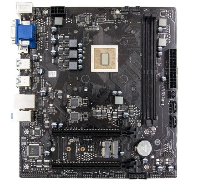
Researchers from Università di Bologna and CINECA, the largest supercomputing center in Italy, have been playing with the concept of developing a RISC-V supercomputer. The team has laid the grounds for the first-ever implementation that demonstrates the capability of the relatively novel ISA to run high-performance computing. To create a supercomputer, you need pieces of hardware that seem like Lego building blocks. Those are called clusters, made from a motherboard, processor, memory, and storage. Italian researchers decided to try and use something different than Intel/AMD solution to the problem and use a processor based on RISC-V ISA. Using SiFive's Freedom U740 SoC as the base, researchers named their RISC-V cluster "Monte Cimone."

Monte Cimone features four dual-board servers, each in a 1U form factor. Each board has a SiFive's Freedom U740 SoC with four U74 cores running up to 1.4 GHz and one S7 management core. In total, eight nodes combine for a total of 32 RISC-V cores. Paired with 16 GB of 64-bit DDR4 memory operating at 1866s MT/s, PCIe Gen 3 x8 bus running at 7.8 GB/s, one gigabit Ethernet port, USB 3.2 Gen 1 interfaces, the system is powered by two 250 Watt PSUs to support future expansion and addition of accelerator cards.

Intel 4 Process Node Detailed, Doubling Density with 20% Higher Performance

Intel's semiconductors nodes have been quite controversial with the arrival of the 10 nm design. Years in the making, the node got delayed multiple times, and only recently did the general public get the first 10 nm chips. Today, at IEEE's annual VLSI Symposium, we get more details about Intel's upcoming nodes, called Intel 4. Previously referred to as a 7 nm process, Intel 4 is the company's first node to use EUV lithography accompanied by various technologies. The first thing when a new process node is discussed is density. Compared to Intel 7, Intel 4 will double the transistor count for the same area and enable 20% higher performing transistors.

Looking at individual transistor size, the new Intel 4 node represents a very tiny piece of silicon that is even smaller than its predecessor. With a Fin Pitch of 30 nm, Contact Gate Poly Pitch of 50 nm between gates, and Minimum Metal Pitch (M0) of 50 nm, the Intel 4 transistor is significantly smaller compared to the Intel 7 cell, listed in the table below. For scaling, Intel 4 provides double the number of transistors in the same area compared to Intel 7. However, this reasoning is applied only to logic. For SRAM, the new PDK provides 0.77 area reduction, meaning that the same SoC built on Intel 7 will not be half the size of Intel 4, as SRAM plays a significant role in chip design. The Intel 7 HP library can put 80 million transistors on a square millimeter, while Intel 4 HP is capable of 160 million transistors per square millimeter.

Intel Core i9-13900 "Raptor Lake" Processor Gets a Preview

Intel is preparing to launch its 13th generation of desktop processors codenamed Raptor Lake. Succeeding Alder Lake, the 13th gen design will implement up to eight P-cores with 16 E-cores manufactured on Intel's improved 7+ technology node. Today, we got a performance preview from SiSoftware that has collected SiSoftware Sandra database scores of Intel Core i9-13900 Raptor Lake-S processor. They present an overview of a few benchmarks. Firstly, the SoC features 36 MB of unified L3 cache versus 30 MB in Alder Lake. With DDR5 memory running up to 5600 MT/s and PCIe 5.0, the SoC features the latest IO and memory standards. The big P-cores now lack AVX-512 and feature 2 MB of L2 cache per core. We see 4 MB of L2 cache for a cluster of small E-cores. An exciting addition to E-cores is the AVX/AVX2 support, which is a first for Atom cores.

Regarding testing, the author has collected a few tests that seemed appropriate to compare to the equivalent Alder Lake model. Starting with ALU/FPU tests that benchmark basic arithmetic tasks, Raptor Lake delivered 33% to 50% improvement over Alder Lake. The Raptor Lake design achieved this with 3.7 GHz P-Core and 2.76 GHz E-Core frequency. In vectorized and SIMD tests, the 13th gen design showed only 5% to 8% improvement over the previous generation. For more benchmarks and accurate results, we have to wait for TechPowerUp's test, which will be coming on the release day.

World's Top Ten IC Design Company Revenue Reached US$39.43 billion in 1Q22, Marvell Growth Rate Tops List, Says TrendForce

According to the latest TrendForce statistics, the top ten IC designers worldwide posted a combined revenue of US$39.43 billion in 1Q22, or 44% growth YoY. Qualcomm, NVIDIA, Broadcom ranked in the top three. After the acquisition of Xilinx, AMD surpassed MediaTek in the fourth position. In addition, according to TrendForce tracking of IC design industry trends, revenue generated by Will Semiconductor and Cirrus Logic was enough to be included in the top ten for the first time.

Benefiting from growth performance in handsets and RF front-end divisions in addition to its IoT and automotive divisions in 1Q22, Qualcomm's quarterly revenue reached US$9.55 billion, or 52% growth YoY, ranking number one in the world. The expanded application of GPUs in data centers boosted this portion of NVIDIA's revenue to 45.4%, surpassing the 45% accounted for by its gaming business, combining for a total revenue of US$7.9 billion, or 53% growth YoY. Broadcom's revenue from semiconductor solutions is substantial, including network chips, broadband communication chips, and storage and bridging chips. Its business has maintained stable sales performance, with revenue reaching US$6.11 billion, or 26% growth YoY. After the addition of Xilinx, AMD's revenue reached US$5.89 billion, or 71% growth YoY. However, even excluding Xilinx, due to strong sales in its enterprise, embedded and semi-customized divisions, AMD's own business revenue still hit an all-time high of US$5.33 billion.

MediaTek Launches First mmWave Chipset for Seamless 5G Smartphone Connectivity

MediaTek today announced the Dimensity 1050 system-on-chip [SoC], its first mmWave 5G chipset that will power the next generation of 5G smartphones with seamless connectivity, displays, gaming and power efficiency. Through dual connectivity using mmWave and sub-6 GHz, the Dimensity 1050 will deliver the speeds and capacity required to provide smartphone users with an incredible experience, even in some of the most densely populated areas. The Dimensity 1050 combines mmWave 5G and sub-6 GHz to fluidly migrate between network bands, and is built on the ultra-efficient TSMC 6 nm production process with an octa-core CPU. Supporting 3CC carrier aggregation on sub-6 (FR1) spectrum and 4CC carrier aggregation on mmWave (FR2) spectrum, the Dimensity 1050 will be capable of delivering up to 53 percent faster speeds and greater reach to smartphones compared to LTE + mmWave aggregation alone. The SoC integrates two premium Arm Cortex-A78 CPUs with speeds reaching 2.5 GHz and the latest Arm Mali-G610 graphics engine.

"The Dimensity 1050, and its combination of sub-6 GHz and mmWave technologies, will deliver end-to-end 5G experiences, uninterrupted connectivity and superior power efficiency to meet everyday user demands," said CH Chen, Deputy General Manager of Wireless Communications Business Unit at MediaTek. "With faster, more reliable connections, and advanced camera technology this chip delivers powerful features to help device makes to differentiate their smartphone product lines." In addition to 5G optimizations, the Dimensity 1050 offers Wi-Fi optimizations alongside MediaTek's HyperEngine 5.0 gaming technology to ensure lower-latency connections with the new tri-band - 2.4 GHz, 5 GHz and 6 GHz - that extends game time and performance. Additionally, high-end UFS 3.1 storage and LPDDR5 memory ensure ultra-fast data streams to accelerate apps, social feeds and faster FPS in games.

Qualcomm Announces Snapdragon 8+ Gen 1 and Snapdragon 7 Gen 1

Qualcomm Technologies, Inc. announced its latest lineup of mobile platforms, Snapdragon 8+ Gen 1 and Snapdragon 7 Gen 1, to power the next generation of premium and high-tier Android smartphones. The Company's newest flagship platform, Snapdragon 8+, is a premium-tier powerhouse delivering power and performance enhancements for the ultimate boost across all on-device experiences. Snapdragon 7 offers a selection of high-end, in-demand features and technologies and enables them for more people around the world. According to the latest findings from Counterpoint Research, IDC, and Strategy Analytics, Qualcomm Technologies is the global leader in premium Android smartphone SoC industry share.

"In the mobile segment, our primary focus is to deliver new, groundbreaking features and technologies to the industry, and for our customers' flagship devices. We implement these features first in our Snapdragon 8-series and then waterfall them down our mobile roadmap," said Christopher Patrick, senior vice president and general manager, mobile handsets, Qualcomm Technologies, Inc. "The new Snapdragon 8+ and 7 Gen 1 both deliver breakthrough user experiences in their respective tiers."

Russia to Use Chinese Zhaoxin x86 Processors Amidst Restrictions to Replace Intel and AMD Designs

Many companies, including Intel and AMD, have stopped product shipments to Russia amidst the war in Ukraine in the past few months. This has left the Russian state without any new processors from the two prominent x86 designers, thus slowing down the country's technological progress. To overcome this issue, it seems like the solution is embedded in the Chinese Zhaoxin x86 CPUs. According to the latest report from Habr, a motherboard designer called Dannie is embedding Chinese Zhaoxin x86 CPUs into motherboards to provide the motherland with an x86-capable processor. More precisely, the company had designed a BX-Z60A micro-ATX motherboard that embeds Zhaoxin's KaiXian KX-6640MA SoC with eight cores based on LuJiaZui microarchitecture. The SoC is clocked at a frequency range of 2.1-2.7 GHz, carries 4 MB of L2 cache, 16 lanes of PCIe 3.0, and has integrated graphics, all in a 25 Watt TDP.

As far as the motherboard is concerned, it supports two DDR4 memory slots, two PCIe x16 connectors, M.2-2280 and M.2-2230 slots, and three SATA III connectors for storage. For I/O you have USB ports, DisplayPort, HDMI, VGA/D-Sub, GbE, 3.5-mm audio, and additional PS/2 ports. This is a pretty decent selection; however, we don't know the pricing structure. A motherboard with KaiXian KX-6640MA SoC like this is certainly not cheap, so we are left to wonder if this will help Russian users deal with the newly imposed restriction on importing US tech.

Nintendo Working on Next-Gen Switch Powered by an NVIDIA SoC

Nintendo could release its next-generation handheld game console, a successor to the crazy-popular Switch, by 2024. This could be powered by an NVIDIA-sourced SoC. NVIDIA recently put up a job listing for a "Game Console Developer Tools Engineer," looking for talent designing the software development applications for the next-generation console. Nintendo is a long-standing customer of NVIDIA chips for its handheld consoles. The next-gen SoC could implement an NVIDIA-designed Arm CPU, and a highly efficient GPU based on the NVIDIA graphics architecture of the time.

MediaTek Unveils New AIoT Platform Stack and Introduces the Genio 1200 AIoT Chip

MediaTek today unveiled its new Genio platform for AIoT devices and introduced the first chip in the Genio family, the Genio 1200 designed for premium AIoT products. MediaTek Genio is a complete platform stack for the AIoT with powerful and ultra- efficient chipsets, open platform software development kits (SDKs) and a developer portal with comprehensive resources and tools. This all-in-one platform makes it easy for brands to develop innovative consumer, enterprise and industrial smart applications at the premium, mid-range and entry levels, and bring these devices to market faster. With MediaTek Genio, customers have access to all the hardware, software and resources needed to go from concept to design and manufacturing.

Customers can choose from a range of Genio chips to suit their product needs, and then use MediaTek's developer resources and the Yocto Linux open platform SDK to customize their designs. MediaTek also makes it easy for customers to access its partners' system hardware and software, and leverage partners' networks and sales channels. By offering an integrated, easy-to-use platform, MediaTek Genio reduces development costs and speeds up time to market, while providing long-term support for operating system updates and security patches that extend the product lifecycle. "Today MediaTek powers the most popular AIoT devices on the market. As the industry enters the next era of innovation, MediaTek's Genio platform delivers flexibility, scalability and development support brands need to cater to the latest market demands," said Jerry Yu, MediaTek Corporate Senior Vice President and General Manager of MediaTek's Computing, Connectivity and Metaverse Business Group. "We look forward to seeing the new user experiences brands bring to life with the Genio 1200 and its powerful AI capability, support for 4K displays and advanced imaging features."

AMD Ryzen 7000U "Phoenix" Processor iGPU Matches RTX 3060 Laptop GPU Performance: Rumor

AMD is planning a massive integrated graphics performance uplift for its next-generation Ryzen 7000U mobile processors. Codenamed "Phoenix," this SoC will feature a CPU based on the "Zen 4" microarchitecture with a higher CPU core count than the Intel alternative of the time; and an iGPU based on the RDNA3 graphics architecture. AMD is planning to endow this with the right combination of a CU count and engine clocks, to result in performance that roughly matches the NVIDIA GeForce RTX 3060 Laptop GPU, a popular performance-segment discrete GPU for notebooks, according to greymon55. Other highlights of "Phoenix" include a DDR5 + LPDDR5 memory interface, and PCI-Express Gen 5. The SoC is expected to be built on the TSMC N5 (5 nm) process, and debut in 2023.

Broadcom Launches its First WiFi 7 Chipsets and corresponding SoC

It appears that 2022 might be the year WiFi 7, or 802.11be as it's also known, launches, despite the fact that the specification isn't set to be ratified until 2024. Broadcom has just unveiled its first set of WiFi 7 radios, as well as accompanying SoC and it looks like the new hardware will bring a big jump in performance under the right circumstances. Broadcom's first WiFi 7 SoC will be known as the BCM4916, which sports a quad core ARMv8 processor. It appears to be a custom Broadcom design that's capable of delivering up to 24 DMIPS of performance, but beyond mentioning that it has 1 MB L2 cache and 64 kB L1 cache, Broadcom doesn't go into any specifics.

The Arm based processor is backed up by what Broadcom calls a Dual Issue Runner Network Processor, or DI-XRDP, which is a packet processor that shuffles the data around between the wired and wireless network interfaces. There's also a crypto coprocessor and Broadcom has added support for Arm TrustZone and Secure Boot, with the prior having support for a trusted execution environment. What stands out with regards to the BCM4916 compared to most current router SoCs is the wide arrange of high-speed connectivity options. For starters, it has no less than four PCIe interfaces of unspecified generation, as well as a native 10 Gbps network interface and as well as the option for two more. In addition to this, it has a further option for a 2.5 Gbps Ethernet interface, as well as a typical four port Gigabit switch built in. A pair of USB 3.2 ports are also part of the chip, but these are likely to be 5 Gbps ports. The SoC also has support for DDR3 and DDR4 memory.

MediaTek Announces First Commercial SoC Support for Dolby Vision IQ

MediaTek has announced it is the first TV SoC vendor to support Dolby Vision IQ with Precision Detail. Precision Detail is a new innovative feature introduced for TVs with Dolby Vision IQ, which will be supported in MediaTek's Pentonic series for 8K and 4K smart TVs. In addition, the Pentonic series will enable TV manufacturers to support features designed for gaming in Dolby Vision along with other advanced capabilities. MediaTek and Dolby collaborated on the implementation of these technologies, which will be available starting in 2H 2022 for TV OEMs to begin adopting.

Joining Dolby's suite of Advanced Imaging technologies available through Dolby Vision IQ, Precision Detail unlocks more from Dolby Vision content by revealing incredible detail in both bright and dark areas. With added texture and depth, images take on a new dimension with astonishing crispness on 8K and 4K smart TVs. In addition to Precision Detail, MediaTek's Intelligent View technology paired with Dolby's latest advancements in imaging technology can process multiple Dolby Vision streams simultaneously. Consumers can now watch different media sources at the same time in Dolby Vision in multiple windows, all in stunning detail.

Oosto Launches Edge-Based Vision AI Appliance to Revolutionize the TCO Calculus of Video Analytics

Oosto announced today the launch of the Oosto Vision AI Appliance, a revolutionary near-edge device that delivers the power and security of Vision AI in a palm-sized device, allowing organizations to protect people, customers and assets more affordably while reducing IT complexity. The Vision AI Appliance is based on the NVIDIA Jetson Xavier NX system on module and is equipped with Oosto's state-of-the-art neural network models for video analytics that are optimized to support low-power devices. Significantly, this was achieved without compromising on superior performance, security or recognition accuracy which historically required compute-intensive GPU processing servers.

This announcement is part of Oosto's ongoing commitment to edge computing. In 2021, the company embedded its Vision AI algorithms on Ambarella's CV2x family of edge AI vision SoCs. Moving the workload to the chip level and to near-edge devices enables organizations to perform real-time video analysis. Significant processing power is required to analyze every frame of a video feed and perform a variety of instant computations to determine if the person entering a building is an authorized employee or on a watchlist (e.g., a VIP or security threat).

Apple Mac Studio Taken Apart, Reveals Giant M1 Ultra SoC

Max Tech performed the first detailed teardown of the Apple Mac Studio, the most powerful Mac since Apple dumped Intel for processors in favor of its own silicon based around high-performance Arm chips built from the ground-up for its own software ecosystem. The M1 Ultra SoC powering the Mac Studio is its most striking piece of technology, with Apple attaching some very tall performance claims not just for its CPU compute performance, but also graphics rendering performance.

The M1 Ultra SoC is physically huge, with roughly similar package size to an AMD EPYC processor in the SP3 package. An integrated heatspreader (IHS) covers almost the entire topside of the package. Things get interesting under the hood. The M1 Ultra is a multi-chip module of two M1 Max dies connected on package using Apple UltraFusion, a coherent fabric interconnect that allows the various components of the two M1 Max dies to access memory controlled by the other die. Speaking of memory, The M1 Ultra features up to 128 GB of LPDDR5 memory that's on-package, This memory is used for the CPU, GPU, as well as the neural processor, and has a combined memory bandwidth of 800 GB/s. The M1 Ultra features up to 20 CPU cores, up to 32 Neural cores, and up to 64 GPU cores (8,192 programmable shaders).

Apple Unveils All-New Mac Studio & Studio Display

Apple today introduced Mac Studio and Studio Display, an entirely new Mac desktop and display designed to give users everything they need to build the studio of their dreams. A breakthrough in personal computing, Mac Studio is powered by M1 Max and the new M1 Ultra, the world's most powerful chip for a personal computer. It is the first computer to deliver an unprecedented level of performance, an extensive array of connectivity and completely new capabilities, in an unbelievably compact design that sits within arm's reach on the desk.

With Mac Studio, users can do things that are not possible on any other desktop, such as rendering massive 3D environments and playing back 18 streams of ProRes video. Studio Display, the perfect complement to Mac Studio, also pairs beautifully with any Mac. It features an expansive 27-inch 5K Retina display, a 12MP Ultra Wide camera with Centre Stage, and a high-fidelity six-speaker sound system with Spatial Audio. Together, Mac Studio and Studio Display transform any workspace into a creative powerhouse. They join Apple's strongest, most powerful Mac line-up ever, and are available to order today, arriving to customers beginning Friday, 18 March.

Apple Unveils M1 Ultra, the World's Most Powerful Chip For a Personal Computer

Apple today announced M1 Ultra, the next giant leap for Apple silicon and the Mac. Featuring UltraFusion — Apple's innovative packaging architecture that interconnects the die of two M1 Max chips to create a system on a chip (SoC) with unprecedented levels of performance and capabilities — M1 Ultra delivers breathtaking computing power to the new Mac Studio while maintaining industry-leading performance per watt.

The new SoC consists of 114 billion transistors, the most ever in a personal computer chip. M1 Ultra can be configured with up to 128 GB of high-bandwidth, low-latency unified memory that can be accessed by the 20-core CPU, 64-core GPU and 32-core Neural Engine, providing astonishing performance for developers compiling code, artists working in huge 3D environments that were previously impossible to render, and video professionals who can transcode video to ProRes up to 5.6x faster than with a 28-core Mac Pro with Afterburner.

TrendForce: DDR3 Consumer DRAM Prices Expected to Rise by 0-5% in 2Q22 Due to Rapidly Shrinking Supply

Intel and AMD will be releasing new CPUs that support DDR5 DRAM solutions for PCs and servers this year. In response, the DRAM industry led by South Korean suppliers is developing solutions to complement the arrival of the new CPUs. In the midst of the gradual shift to DDR5, DRAM suppliers will also scale back the supply of DDR3 solutions, according to TrendForce's latest investigations. With Korean suppliers accelerating their withdrawal from DDR3 production, Taiwanese suppliers yet to kick off mass production using newly installed capacities, and Chinese suppliers falling short of their expected yield rate, the global supply of DDR3 solutions will undergo an impending decline. With respect to the demand side, however, not only has the supply of networking chips been ramping up, but material shortage issues are also gradually easing. As such, buyers are now procuring DDR3 solutions ahead of time, resulting in a tight supply and demand situation in the DDR3 market. TrendForce therefore expects DDR3 DRAM prices to recover from a bearish first quarter and undergo a 0-5% QoQ increase in 2Q22.

MediaTek Launches Dimensity 8000 5G Chip Series for Premium 5G Smartphones

MediaTek today launched the Dimensity 8100 and Dimensity 8000 system-on-chips (SoCs) to bring flagship level technology - connectivity, displays, gaming, multimedia and imaging features - to premium 5G smartphones. Both chips borrow the advanced technology from MediaTek's powerful flagship Dimensity 9000 platform and package it into the new Dimensity 8000 series which is built on the ultra-efficient TSMC 5 nm production process with an octa-core CPU. The Dimensity 8100 integrates four premium Arm Cortex-A78 cores with speeds reaching 2.85 GHz, and the Dimensity 8000 has four Cortex-A78 cores operating at up to 2.75 GHz.

"You could say the MediaTek Dimensity 8000 series is the little brother to our flagship Dimensity 9000 chip. Meaning it brings flagship grade features and next level energy efficiency to the premium smartphone market," said CH Chen, Deputy General Manager of MediaTek's Wireless Communications Business Unit. Both chips combine an Arm Mali-G610 MC6 GPU with MediaTek's HyperEngine 5.0 gaming technologies for exceptional power-efficiency that extends play time, and best-in-class frame rates - 170fps for the Dimensity 8100 and 140fps for the Dimensity 8000. Quad-channel LPDDR5 memory and UFS 3.1 storage ensure ultra-fast data streams.

Nintendo Switch Pro Reportedly Surfaces in NVIDIA Leak

The recently leaked NVIDIA DLSS source code appears to contain several references to an upcoming Nintendo Switch product with files such as "nvndlss.cpp", "nvn_dlss.cpp", and "nvn_dlss_backend.h" listed which reputable leaker @kopite7kimi believes belongs to an upcoming Nintendo Switch model with a new SoC. The files are all found within a folder titled NVN2 which is likely referring to the successor of the NVN graphics API written by NVIDIA for the original Nintendo Switch.

These files allegedly contain references to an 8 nm T239 chip that looks extremely likely to be designated for the Nintendo Switch Pro based on Ampere with ray tracing support and DLSS 2.2 according to @NWPlayer123. This supports previous rumors that pointed to a Nintendo Switch Pro featuring a new NVIDIA processor with DLSS 2.0 support.

Qualcomm Expands Snapdragon Compute Ecosystem for the Next-Generation of Enterprise-Grade PCs

Today, during Mobile World Congress 2022, Qualcomm Incorporated President and Chief Executive Officer, Cristiano Amon highlighted how Qualcomm Technologies, Inc. is continuing to bring best-in-case experiences to enterprise PCs and drive the convergence of the PC and mobile to increase productivity, connectivity, and security from anywhere. During last month's Consumer Electronics Show, the Company announced that over 200 enterprise customers were testing or deploying Windows 11 on Snapdragon laptops and 2-in-1 devices. Today, Amon outlined how strategic relationships with Microsoft, Lenovo, and many other ecosystem leaders are helping deliver the next generation of enterprise-ready PCs, powered by Snapdragon. Utilizing its global relationships, Qualcomm Technologies continues to lead the PC industry's inevitable transition to innovative and modern solutions from the portfolio of Snapdragon compute platforms.
Quotes from key collaborators that Qualcomm Technologies is working with to drive innovation for always on, always connected enterprise PCs through Snapdragon Compute Platforms can be found here.

Intel Launches Xeon D Processor Built for the Network and Edge

Today, ahead of MWC Barcelona 2022, Intel launched new Intel Xeon D processors: the D-2700 and the D-1700. They are Intel's newest system-on-chip (SoC) built for the software-defined network and edge, with integrated AI and crypto acceleration, built-in Ethernet, support for Intel Time Coordinated Computing (Intel TCC) and Time Sensitive Networking (TSN), and industrial-class reliability. New Intel Xeon D processors extend compute with acceleration beyond the core data center, generating a better overall experience for key network and edge usages and workloads.

"As the industry enters a world of software-defined everything, Intel is delivering programmable platforms for networking and the edge to enable one of the most significant transformations our industry has ever seen. The new Intel Xeon D processor is built for this. Based on the proven and trusted Intel architecture, this processor is designed for a range of use cases to unleash innovation across the network and edge," said Dan Rodriguez, Intel corporate vice president, Network & Edge Group, general manager of the Network Platforms Group.

Intel Makes Jilted Reference to Apple in its Internal "Arrow Lake" Slide

Intel is designing a "Halo" SKU of a future generation of mobile processors with a goal to match Apple's in-house silicon of the time. Slated for tape-out some time in 2023, with mass-production expected in 2024, the 15th Generation Core "Arrow Lake-P Halo" processor is being designed specifically to compete with Apple's "premium 14-inch laptop" (presumably the MacBook Pro) that the company could have around 2024, based on an in-house Apple silicon. This is to essentially tell its notebook partners that they will have an SoC capable of making their devices in the class truly competitive. Apple relies on a highly scaled out Arm-based SoC based on in-house IP blocks, with a software that's closely optimized for it. Intel's effort appears to chase down its performance and efficiency.

The Core "Arrow Lake" microarchitecture succeeds the 14th Gen "Meteor Lake." It is a multi-chip module (MCM) of three distinct dies built on different fabrication nodes, in line with the company's IDM 2.0 strategy. These nodes are Intel 4 (comparable to TSMC N7 or N6), Intel 20A (comparable to TSMC N5), and an "external" 3 nm-class node that's just the TSMC N3. The compute tile, or the die which houses the CPU cores, combines a hybrid CPU setup of 6 P-cores, and 8 E-cores. The performance cores are likely successors of the "Redwood Cove" P-cores powering the "Meteor Lake" compute tiles. Intel appears to be using one kind of E-cores across two generations (eg: Gracemont across Alder Lake and Raptor Lake). If this is any indication, Arrow Lake could continue to use "Crestmont" E-cores. Things get interesting with the Graphics tile.

Samsung RDNA2-based Exynos 2200 GPU Performance Significantly Worse than Snapdragon 8 Gen1, Both Power Galaxy S22 Ultra

The Exynos 2200 SoC powering the Samsung Galaxy S22 Ultra in some regions such as the EU, posts some less-than-stellar graphics performance numbers, for all the hype around its AMD-sourced RDNA2 graphics solution, according to an investigative report by Erdi Özüağ, aka "FX57." Samsung brands this RDNA2-based GPU as the Samsung Xclipse 920. Further, Özüağ's testing found that the Exynos 2200 is considerably slower than the Qualcomm Snapdragon 8 Gen 1 powering the S22 Ultra in certain other regions, including the US and India. He has access to both kinds of the S22 Ultra.

In the UL Benchmarks 3DMark Wildlife test, the Exynos 2200 posted a score of 6684 points, compared to 9548 points by the Snapdragon 8 Gen 1 (a difference of 42 percent). What's even more interesting, is that the Exynos 2200 is barely 7 percent faster than the previous-gen Exynos 2100 (Arm Mali GPU) powering the S21 Ultra, which scored 6256 points. The story repeats with the GFXBench "Manhattan" off-screen render benchmark. Here, the Snapdragon 8 Gen 1 is 30 percent faster than the Exynos 2200, which performs on-par with the Exynos 2100. Find a plethora of other results in the complete review comparing the two flavors of the S22 Ultra.

AMD Completes Acquisition of Xilinx

AMD (NASDAQ: AMD) today announced the completion of its acquisition of Xilinx in an all-stock transaction. The acquisition, originally announced on October 27, 2020, creates the industry's high-performance and adaptive computing leader with significantly expanded scale and the strongest portfolio of leadership computing, graphics and adaptive SoC products. AMD expects the acquisition to be accretive to non-GAAP margins, non-GAAP EPS and free cash flow generation in the first year.

"The acquisition of Xilinx brings together a highly complementary set of products, customers and markets combined with differentiated IP and world-class talent to create the industry's high-performance and adaptive computing leader," said AMD President and CEO Dr. Lisa Su. "Xilinx offers industry-leading FPGAs, adaptive SoCs, AI engines and software expertise that enable AMD to offer the strongest portfolio of high-performance and adaptive computing solutions in the industry and capture a larger share of the approximately $135 billion market opportunity we see across cloud, edge and intelligent devices."

AMD Receives All Regulatory Approvals to Acquire Xilinx

AMD (NASDAQ: AMD) today announced that it has received approval from all necessary authorities to proceed with the acquisition of Xilinx, Inc. (NASDAQ: XLNX). With the exception of the remaining customary closing conditions, all conditions to the transaction closing have been satisfied and the company expects the transaction to close on or about February 14, 2022.

AMD announced its intention to acquire Xilinx in an all-stock transaction on October 27, 2020. The transaction brings together two industry leaders with complementary product portfolios and customers, combining CPUs, GPUs, FPGAs, Adaptive SoCs and deep software expertise to enable leadership computing platforms for cloud, edge and intelligent end devices.
Return to Keyword Browsing
Jun 1st, 2024 18:38 EDT change timezone

New Forum Posts

Popular Reviews

Controversial News Posts