News Posts matching #Micron

Return to Keyword Browsing

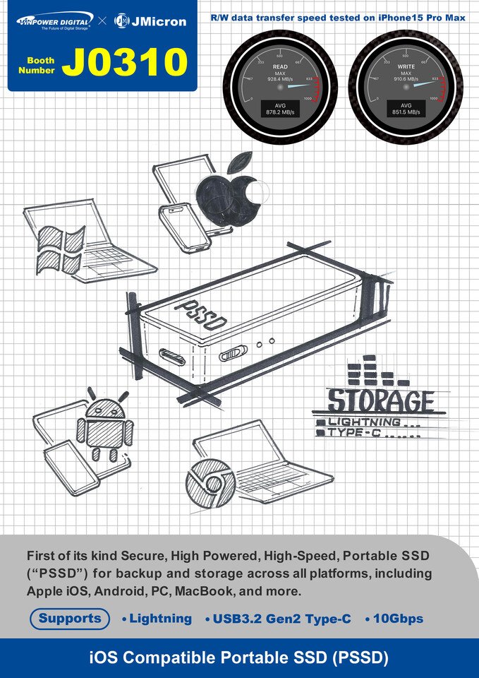
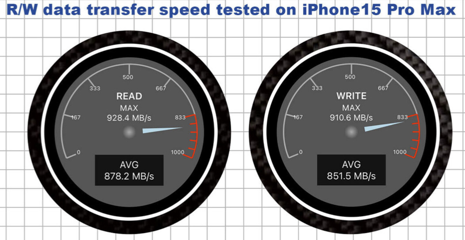
Growing Demand for High-Capacity Storage Propels Enterprise SSD Revenue Up by Over 60% in 1Q24

TrendForce reports that a reduction in supplier production has led to unmet demand for high-capacity orders since 4Q23. Combined with procurement strategies aimed at building low-cost inventory, this has driven orders and significantly boosted enterprise SSD revenue, which reached US$3.758 billion in 1Q24—a staggering 62.9% QoQ increase.

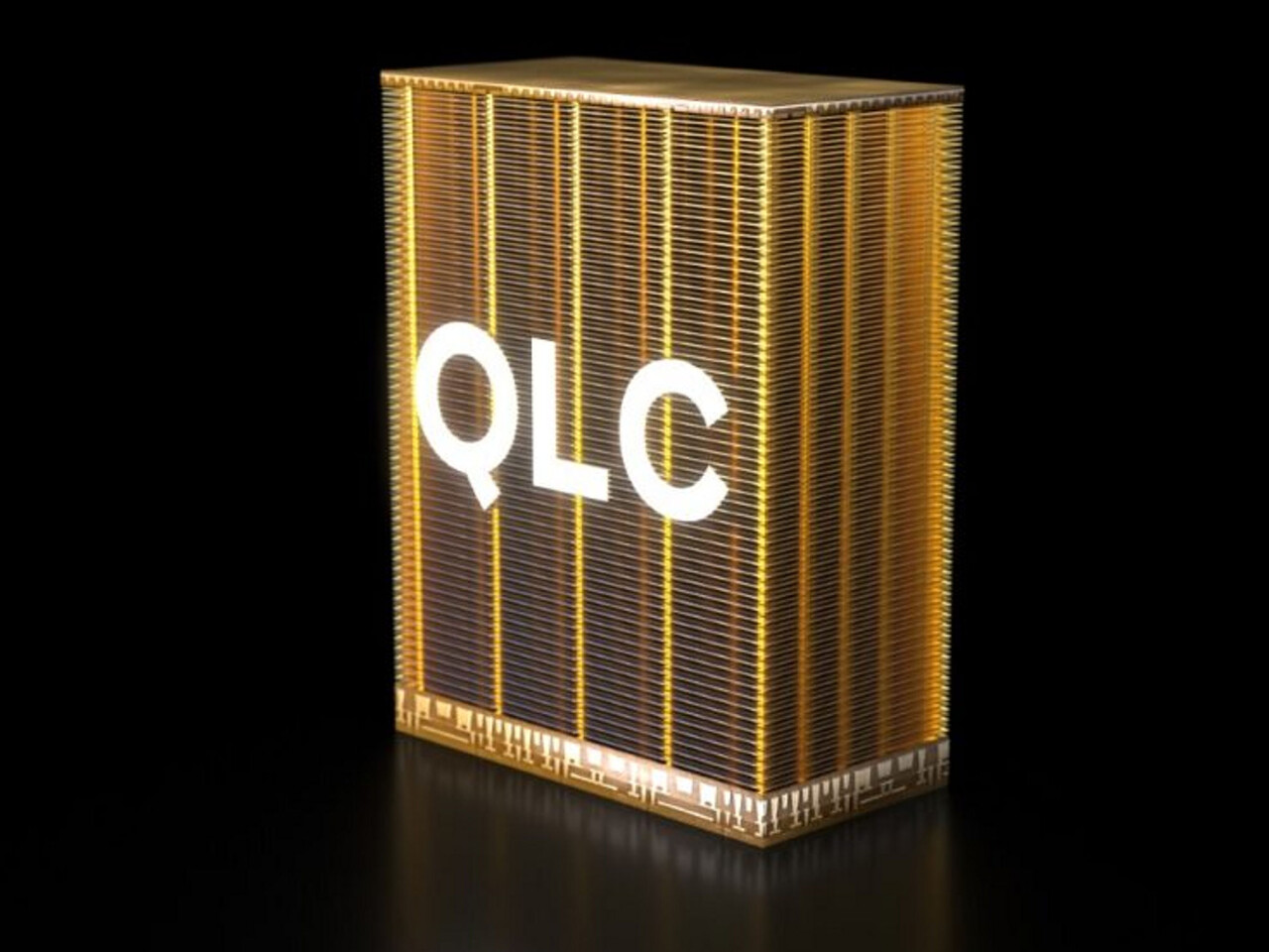
TrendForce further highlights that demand for high-capacity, driven by AI servers, has surged. North American clients increasingly adopt high-capacity QLC SSDs to replace HDDs, leading to over 20% growth in Q2 enterprise SSD bit procurement. This has also driven up Q2 enterprise SSD contract prices by more than 20%, with revenue expected to grow by another 20%.

Micron First to Achieve Qualification Sample Milestone to Accelerate Ecosystem Adoption of CXL 2.0 Memory

Micron Technology, a leader in innovative data center solutions, today announced it has achieved its qualification sample milestone for the Micron CZ120 memory expansion modules using Compute Express Link (CXL). Micron is the first in the industry to achieve this milestone, which accelerates the adoption of CXL solutions within the data center to tackle the growing memory challenges stemming from existing data-intensive workloads and emerging artificial intelligence (AI) and machine learning (ML) workloads.

Using a new and emerging CXL standard, the CZ120 required substantial hardware testing for reliability, quality and performance across CPU providers and OEMs, along with comprehensive software testing for compatibility and compliance with OS and hypervisor vendors. This achievement reflects the collaboration and commitment across the data center ecosystem to validate the advantages of CXL memory. By testing the combined products for interoperability and compatibility across hardware and software, the Micron CZ120 memory expansion modules satisfy the rigorous standards for reliability, quality and performance required by customers' data centers.

Micron DRAM Production Plant in Japan Faces Two-Year Delay to 2027

Last year, Micron unveiled plans to construct a cutting-edge DRAM factory in Hiroshima, Japan. However, the project has faced a significant two-year delay, pushing back the initial timeline for mass production of the company's most advanced memory products. Originally slated to begin mass production by the end of 2025, Micron now aims to have the new facility operational by 2027. The complexity of integrating extreme ultraviolet lithography (EUV) equipment, which enables the production of highly advanced chips, has contributed to the delay. The Hiroshima plant will produce next-generation 1-gamma DRAM and high-bandwidth memory (HBM) designed for generative AI applications. Micron expects the HBM market, currently dominated by rivals SK Hynix and Samsung, to experience rapid growth, with the company targeting a 25% market share by 2025.

The project is expected to cost between 600 and 800 billion Japanese yen ($3.8 to $5.1 billion), with Japan's government covering one-third of the cost. Micron has received a subsidy of up to 192 billion yen ($1.2 billion) for construction and equipment, as well as a subsidy to cover half of the necessary funding to produce HBM at the plant, amounting to 25 billion yen ($159 million). Despite the delay, the increased investment in the factory reflects Micron's commitment to advancing its memory technology and capitalizing on the growing demand for HBM. An indication of that is the fact that customers have pre-ordered 100% of the HBM capacity for 2024, not leaving a single HBM die unused.

Malaysia Plans to Build the Largest Integrated Circuit Design Park in Southeast Asia

Malaysia is firmly positioning itself as a hub for semiconductor investment, with Prime Minister Anwar Ibrahim stating the country aims to attract over $100 billion in investment into the industry. This aligns with recent trends in the region, such as China's announcement of a massive $47.5 billion investment fund or Micron's plans to build a new chip factory in Hiroshima, Japan by the end of 2027.

As a major player accounting for 13% of global chip testing and packaging, Malaysia has benefited from strong investments by Intel ($7 billion for an advanced packaging plant) and Infineon ($5.4 billion to expand its power chip plant). The country now hopes around 10 local companies will make substantial investments in new facilities focused on chip design and advanced packaging. To support this goal, the Malaysian government plans to allocate $5.3 billion in fiscal backing, along with tax breaks and subsidies. It is targeting these investments to generate revenues between $210 million and $1 billion for the semiconductor industry in Malaysia.
Microchips

NAND Flash Industry Revenue Grew 28.1% in 1Q24, Growth Expected to Continue into Q2

TrendForce reports that adoption of enterprise SSDs by AI servers began in February, which subsequently led to large orders. Additionally, PC and smartphone customers have been increasing their inventory levels to manage rising prices. This trend drove up NAND Flash prices and shipment levels in 1Q24 and boosted quarterly revenue by 28.1% to US$14.71 billion.

There were significant changes in market rankings this quarter, with Micron overtaking Western Digital to claim the fourth spot. Micron benefited from slightly lower prices and shipments than its competitors in 4Q23, resulting in a 51.2% QoQ revenue growth to $1.72 billion in 1Q24—the highest among its peers.

NVIDIA Reportedly Having Issues with Samsung's HBM3 Chips Running Too Hot

According to Reuters, NVIDIA is having some major issues with Samsung's HBM3 chips, as NVIDIA hasn't managed to finalise its validations of the chips. Reuters are citing multiple sources that are familiar with the matter and it seems like Samsung is having some serious issues with its HMB3 chips if the sources are correct. Not only do the chips run hot, which itself is a big issue due to NVIDIA already having issues cooling some of its higher-end products, but the power consumption is apparently not where it should be either. Samsung is said to have tried to get its HBM3 and HBM3E parts validated by NVIDIA since sometime in 2023 according to Reuter's sources, which suggests that there have been issues for at least six months, if not longer.

The sources claim there are issues with both the 8- and 12-layer stacks of HMB3E parts from Samsung, suggesting that NVIDIA might only be able to supply parts from Micron and SK Hynix for now, the latter whom has been supplying HBM3 chips to NVIDIA since the middle of 2022 and HBM3E chips since March of this year. It's unclear if this is a production issue at Samsung's DRAM Fabs, a packaging related issue or something else entirely. The Reuter's piece goes on to speculating about Samsung not having had enough time to develop its HBM parts compared its competitors and that it's a rushed product, but Samsung issued a statement to the publication that it's a matter of customising the product for its customer's needs. Samsung also said that it's "the process of optimising its products through close collaboration with customers" without going into which customer(s). Samsung issued a further statement saying that "claims of failing due to heat and power consumption are not true" and that testing was going as expected.

JMicron and Vinpower will Introduce the World's First 10Gbps Portable SSD Compatible with Apple iOS at Computex

JMicron Technology Corporation, in collaboration with Vinpower, Inc., have developed the first of its kind Enhanced 10Gbps Portable SSD (PSSD), using the collaboratively developed iVP817 IC Chip, that's compatible with Apple iOS devices supporting the iPhone iAP2. The PSSD offers super-fast Read/Write (R/W) data transfer speeds and is the first of its kind to provide Secure, High Powered, High-Speed backup and storage across all computing platforms, which includes the Apple iOS platform, as well as Android, PC, MacBook, Chromebook and more. While the R/W transfer speeds for USB flash storage devices compatible with smartphones and tablets typically range from 20 MB/sec to 80 MB/sec, the enhanced PSSD achieved verifiable R/W transfer speeds at more than 800 MB/sec with an iPhone 15Pro and 15Pro Max. That means, when using the enhanced PSSD with Vinpower's iAP2 based App, one could backup a 10 GB video, from an iPhone 15Pro or 15Pro Max, in around 12 seconds. On top of that, the PSSD will accommodate a range of NVMe SSD with varying form factor lengths and capacities up to and exceeding 8 TB of secure storage.

JMicron is a leading IC design company specialized in high-speed data and signal interfaces bridge controllers including NVMe to USB bridges, while Vinpower is a leader in designing IC chip firmware, circuit design, and manufacturing Apple iOS backup and storage devices and related Apps. The two companies recognized the enormous untapped market potential for a new solution that can perform smooth, fast, and secure data transfer and backup for portable mobile devices, especially for the Apple iOS platform, such as iPhones and iPads.

HBM3e Production Surge Expected to Make Up 35% of Advanced Process Wafer Input by End of 2024

TrendForce reports that the three largest DRAM suppliers are increasing wafer input for advanced processes. Following a rise in memory contract prices, companies have boosted their capital investments, with capacity expansion focusing on the second half of this year. It is expected that wafer input for 1alpha nm and above processes will account for approximately 40% of total DRAM wafer input by the end of the year.

HBM production will be prioritized due to its profitability and increasing demand. However, limited yields of around 50-60% and a wafer area 60% larger than DRAM products mean a higher proportion of wafer input is required. Based on the TSV capacity of each company, HBM is expected to account for 35% of advanced process wafer input by the end of this year, with the remaining wafer capacity used for LPDDR5(X) and DDR5 products.

TSMC Unveils Next-Generation HBM4 Base Dies, Built on 12 nm and 5 nm Nodes

During the European Technology Symposium 2024, TSMC has announced its readiness to manufacture next-generation HBM4 base dies using both 12 nm and 5 nm nodes. This significant development is expected to substantially improve the performance, power consumption, and logic density of HBM4 memory, catering to the demands of high-performance computing (HPC) and artificial intelligence (AI) applications. The shift from a traditional 1024-bit interface to an ultra-wide 2048-bit interface is a key aspect of the new HBM4 standard. This change will enable the integration of more logic and higher performance while reducing power consumption. TSMC's N12FFC+ and N5 processes will be used to produce these base dies, with the N12FFC+ process offering a cost-effective solution for achieving HBM4 performance and the N5 process providing even more logic and lower power consumption at HBM4 speeds.

The company is collaborating with major HBM memory partners, including Micron, Samsung, and SK Hynix, to integrate advanced nodes for HBM4 full-stack integration. TSMC's base die, fabricated using the N12FFC+ process, will be used to install HBM4 memory stacks on a silicon interposer alongside system-on-chips (SoCs). This setup will enable the creation of 12-Hi (48 GB) and 16-Hi (64 GB) stacks with per-stack bandwidth exceeding 2 TB/s. TSMC's collaboration with EDA partners like Cadence, Synopsys, and Ansys ensures the integrity of HBM4 channel signals, thermal accuracy, and electromagnetic interference (EMI) in the new HBM4 base dies. TSMC is also optimizing CoWoS-L and CoWoS-R for HBM4 integration, meaning that massive high-performance chips are already utilizing this technology and getting ready for volume manufacturing.

Micron Delivers Crucial LPCAMM2 with LPDDR5X Memory for the New AI-Ready Lenovo ThinkPad P1 Gen 7 Workstation

Micron Technology, Inc., today announced the availability of Crucial LPCAMM2, the disruptive next-generation laptop memory form factor that features LPDDR5X mobile memory to level up laptop performance for professionals and creators. Consuming up to 58% less active power and with a 64% space savings compared to DDR5 SODIMMs, LPCAMM2 delivers higher bandwidth and dual-channel support with a single module. LPCAMM2 is an ideal high-performance memory solution for handling AI PC and complex workloads and is compatible with the powerful and versatile Lenovo ThinkPad P1 Gen 7 mobile workstations.

"LPCAMM2 is a game-changer for mobile workstation users who want to enjoy the benefits of the latest mobile high performance memory technology without sacrificing superior performance, upgradeability, power efficiency or space," said Jonathan Weech, senior director of product marketing for Micron's Commercial Products Group. "With LPCAMM2, we are delivering a future-proof memory solution, enabling faster speeds and longer battery life to support demanding creative and AI workloads."

Micron First to Ship Critical Memory for AI Data Centers

Micron Technology, Inc. (Nasdaq: MU), today announced it is leading the industry by validating and shipping its high-capacity monolithic 32Gb DRAM die-based 128 GB DDR5 RDIMM memory in speeds up to 5,600 MT/s on all leading server platforms. Powered by Micron's industry-leading 1β (1-beta) technology, the 128 GB DDR5 RDIMM memory delivers more than 45% improved bit density, up to 22% improved energy efficiency and up to 16% lower latency over competitive 3DS through-silicon via (TSV) products.

Micron's collaboration with industry leaders and customers has yielded broad adoption of these new high-performance, large-capacity modules across high-volume server CPUs. These high-speed memory modules were engineered to meet the performance needs of a wide range of mission-critical applications in data centers, including artificial intelligence (AI) and machine learning (ML), high-performance computing (HPC), in-memory databases (IMDBs) and efficient processing for multithreaded, multicore count general compute workloads. Micron's 128 GB DDR5 RDIMM memory will be supported by a robust ecosystem including AMD, Hewlett Packard Enterprise (HPE), Intel, Supermicro, along with many others.

Enthusiast Transforms QLC SSD Into SLC With Drastic Endurance and Performance Increase

A few months ago, we covered proof of overclocking an off-the-shelf 2.5-inch SATA III NAND Flash SSD thanks to Gabriel Ferraz, Computer Engineer and TechPowerUp's SSD database maintainer. Now, he is back with another equally interesting project of modifying a Quad-Level Cell (QLC) SATA III SSD into a Single-Level Cell (SLC) SATA III SSD. Using the Crucial BX500 512 GB SSD, he aimed at transforming the QLC drive into a more endurant and higher-performance SLC. Silicon Motion SM2259XT2 powers the drive of choice with a single-core ARC 32-bit CPU clocked at 550 MHz and two channels running at 800 MT/s (400 MHz) without a DRAM cache. This particular SSD uses four NAND Flash dies from Micron with NY240 part numbers. Two dies are controlled per channel. These NAND Flash dies were designed to operate at 1,600 MT/s (800 MHz) but are limited to only 525 MT/s in this drive in the real world.

The average endurance of these dies is 1,500 P/E cycles in NANDs FortisFlash and about 900 P/E cycles in Mediagrade. Transforming the same drive in the pSLC is bumping those numbers to 100,000 and 60,000, respectively. However, getting that to work is the tricky part. To achieve this, you have to download MPtools for the Silicon Motion SM2259XT2 controller from the USBdev.ru website and find the correct die used in the SSD. Then, the software is modified carefully, and a case-sensitive configuration file is modified to allow for SLC mode, which forces the die to run as a SLC NAND Flash die. Finally, firmware folder must be reached and files need to be moved arround in a way seen in the video.

Micron to Receive US$6.1 Billion in CHIPS and Science Act Funding

Micron Technology, Inc., one of the world's largest semiconductor companies and the only U.S.-based manufacturer of memory, and the Biden-Harris Administration today announced that they have signed a non-binding Preliminary Memorandum of Terms (PMT) for $6.1 billion in funding under the CHIPS and Science Act to support planned leading-edge memory manufacturing in Idaho and New York.

The CHIPS and Science Act grants of $6.1 billion will support Micron's plans to invest approximately $50 billion in gross capex for U.S. domestic leading-edge memory manufacturing through 2030. These grants and additional state and local incentives will support the construction of one leading-edge memory manufacturing fab to be co-located with the company's existing leading-edge R&D facility in Boise, Idaho and the construction of two leading-edge memory fabs in Clay, New York.

Micron First to Production of 200+ Layer QLC NAND in Client and Data Center

Micron Technology, Inc., today demonstrated its continued NAND technology leadership by announcing that its 232-layer QLC NAND is now in mass production and shipping in select Crucial SSDs, in volume production to enterprise storage customers and sampling to OEM PC manufacturers in the Micron 2500 NMVe SSD.

Micron 232-layer QLC NAND delivers unparalleled performance for use cases across mobile, client, edge and data center storage by leveraging these important capabilities:
  • Industry-leading bit-density, up to 28% more compact than leading competitors' latest products
  • Industry-leading NAND I/O speeds of 2400 MT/s, a 50% improvement over the prior generation
  • 24% better read performance over the prior generation
  • 31% better programming performance over the prior generation

DRAM Manufacturers Gradually Resume Production, Impact on Total Q2 DRAM Output Estimated to Be Less Than 1%

Following in the wake of an earthquake that struck on April 3rd, TrendForce undertook an in-depth analysis of its effects on the DRAM industry, uncovering a sector that has shown remarkable resilience and faced minimal interruptions. Despite some damage and the necessity for inspections or disposal of wafers among suppliers, the facilities' strong earthquake preparedness of the facilities has kept the overall impact to a minimum.

Leading DRAM producers, including Micron, Nanya, PSMC, and Winbond had all returned to full operational status by April 8th. In particular, Micron's progression to cutting-edge processes—specifically the 1alpha and 1beta nm technologies—is anticipated to significantly alter the landscape of DRAM bit production. In contrast, other Taiwanese DRAM manufacturers are still working with 38 and 25 nm processes, contributing less to total output. TrendForce estimates that the earthquake's effect on DRAM production for the second quarter will be limited to a manageable 1%.

Micron Debuts World's First Quad-Port SSD to Accelerate Data-Rich Autonomous and AI-Enabled Workloads

Micron Technology, Inc., today announced it is sampling the automotive-grade Micron 4150AT SSD, the world's first quad-port SSD, capable of interfacing with up to four systems on chips (SoCs) to centralize storage for software-defined intelligent vehicles. The Micron 4150AT SSD combines market-leading features such as single-root input/output virtualization (SR-IOV), a PCIe Generation 4 interface and ruggedized automotive design. With these features, the automotive-grade SSD provides the ecosystem with data center-level flexibility and power.

"As storage requirements race to keep up with rich in-vehicle experiences featuring AI and advanced algorithms for higher levels of autonomous safety, this era demands a new paradigm for automotive storage to match," said Michael Basca, Micron vice president of embedded products and systems. "Building on our collaboration with the innovators redefining next-generation automotive architectures, Micron has reimagined storage from the ground up to deliver the world's first quad-port SSD - the Micron 4150AT - which provides the industry flexibility and horsepower to roll out the transformative technologies on the horizon."

Micron Provides Update Following Earthquake in Taiwan

Micron Technology, Inc. (Nasdaq: MU) today reported that following the earthquake that struck Taiwan on April 3, 2024, all of Micron's team members have been accounted for and reported to be safe. Our thoughts are with those affected and their families. We are evaluating impact to our operations and supply chain. We will communicate changes to delivery commitments to our customers after this evaluation is completed.

Micron Reports Results for Second Quarter of Fiscal 2024

Micron Technology, Inc. today announced results for its second quarter of fiscal 2024, which ended February 29, 2024.

Fiscal Q2 2024 highlights
  • Revenue of $5.82 billion versus $4.73 billion for the prior quarter and $3.69 billion for the same period last year
  • GAAP net income of $793 million, or $0.71 per diluted share
  • Non-GAAP net income of $476 million, or $0.42 per diluted share
  • Operating cash flow of $1.22 billion versus $1.40 billion for the prior quarter and $343 million for the same period last year
"Micron delivered fiscal Q2 results with revenue, gross margin and EPS well above the high-end of our guidance range - a testament to our team's excellent execution on pricing, products and operations," said Sanjay Mehrotra, President and CEO of Micron Technology. "Our preeminent product portfolio positions us well to deliver a strong fiscal second half of 2024. We believe Micron is one of the biggest beneficiaries in the semiconductor industry of the multi-year opportunity enabled by AI."

Kioxia and WD Elevate Capacity Utilization, Pushing NAND Flash Supply Growth to 10.9%

TrendForce reports that anticipation of NAND Flash price hikes into Q2 has motivated certain suppliers to minimize losses and lower costs in hopes of returning to profitability this year. Kioxia and WD led the charge from March, boosting their capacity utilization rates to nearly 90%—a move not widely adopted by their competitors.

TrendForce points out that to meet the demand surge in the second half of the year, especially given Kioxia and Western Digital's currently low inventory, the production increase is mainly targeting 112-layer and select 2D products. This strategy is expected not only to secure profitability within the year but also to contribute to a projected 10.9% rise in the annual NAND Flash industry supply bit growth rate for 2024.

MemVerge and Micron Boost NVIDIA GPU Utilization with CXL Memory

MemVerge, a leader in AI-first Big Memory Software, has joined forces with Micron to unveil a groundbreaking solution that leverages intelligent tiering of CXL memory, boosting the performance of large language models (LLMs) by offloading from GPU HBM to CXL memory. This innovative collaboration is being showcased in Micron booth #1030 at GTC, where attendees can witness firsthand the transformative impact of tiered memory on AI workloads.

Charles Fan, CEO and Co-founder of MemVerge, emphasized the critical importance of overcoming the bottleneck of HBM capacity. "Scaling LLM performance cost-effectively means keeping the GPUs fed with data," stated Fan. "Our demo at GTC demonstrates that pools of tiered memory not only drive performance higher but also maximize the utilization of precious GPU resources."

NAND Flash Market Landscape to Change, Reports TrendForce

With the effective reduction of production by suppliers, the price of memory is rebounding, and the semiconductor memory market finally shows signs of recovery. From the perspective of market dynamics and demand changes, NAND Flash, as one of the two major memory products, is experiencing a new round of changes. Since 3Q23, NAND Flash chip prices have been on the rise for several consecutive months. TrendForce believes that, under the precondition of a conservative market demand prospect for 2024, chip price trends will depend on suppliers' production capacity utilization.

There have been frequent developments in the NAND flash memory industry chain, with some manufacturers indicating a willingness to raise prices or increase production capacity utilization. Wallace C. Kou, General Manager of NAND Flash Supplier SIMO, stated that prices for the second quarter of NAND Flash have already been settled down, which will increase by 20%; some suppliers have started to make profits in the first quarter, and most suppliers will earn money after the second quarter.

NVIDIA's Selection of Micron HBM3E Supposedly Surprises Competing Memory Makers

SK Hynix believes that it leads the industry with the development and production of High Bandwidth Memory (HBM) solutions, but rival memory manufacturers are working hard on equivalent fifth generation packages. NVIDIA was expected to select SK Hynix as the main supplier of HBM3E parts for utilization on H200 "Hopper" AI GPUs, but a surprise announcement was issued by Micron's press team last month. The American firm revealed that HBM3E volume production had commenced: ""(our) 24 GB 8H HBM3E will be part of NVIDIA H200 Tensor Core GPUs, which will begin shipping in the second calendar quarter of 2024. This milestone positions Micron at the forefront of the industry, empowering artificial intelligence (AI) solutions with HBM3E's industry-leading performance and energy efficiency."

According to a Korea JoongAng Daily report, this boast has reportedly "shocked" the likes of SK Hynix and Samsung Electronics. They believe that Micron's: "announcement was a revolt from an underdog, as the US company barely held 10 percent of the global market last year." The article also points out some behind-the-scenes legal wrangling: "the cutthroat competition became more evident when the Seoul court sided with SK Hynix on Thursday (March 7) by granting a non-compete injunction to prevent its former researcher, who specialized in HBM, from working at Micron. He would be fined 10 million won for each day in violation." SK Hynix is likely pinning its next-gen AI GPU hopes on a 12-layer DRAM stacked HBM3E product—industry insiders posit that evaluation samples were submitted to NVIDIA last month. The outlook for these units is said to be very positive—mass production could start as early as this month.

JEDEC Agrees to Relax HBM4 Package Thickness

JEDEC is currently presiding over standards for 6th generation high bandwidth memory (AKA HBM4)—the 12 and 16-layer DRAM designs are expected to reach mass production status in 2026. According to a ZDNET South Korea report, involved manufacturers are deliberating over HBM4 package thicknesses—allegedly, decision makers have settled on 775 micrometers (μm). This is thicker than the previous generation's measurement of 720 micrometers (μm). Samsung Electronics, SK Hynix and Micron are exploring "hybrid bonding," a new packaging technology—where onboard chips and wafers are linked directly to each other. Hybrid bonding is expected to be quite expensive to implement, so memory makers are carefully considering whether HBM4 warrants its usage.

ZDNET believes that JEDEC's agreement—settling on 775 micrometers (μm) for 12-layer and 16-layer stacked HBM4—could have: "a significant impact on the future packaging investment trends of major memory manufacturers. These companies have been preparing a new packaging technology, hybrid bonding, keeping in mind the possibility that the package thickness of HBM4 will be limited to 720 micrometers. However, if the package thickness is adjusted to 775 micrometers, 16-layer DRAM stacking HBM4 can be sufficiently implemented using existing bonding technology." A revised schedule could delay the rollout of hybrid bonding—perhaps pushed back to coincide with a launch of seventh generation HBM. The report posits that Samsung Electronics, SK Hynix and Micron memory engineers are about to focus on the upgrading of existing bonding technologies.

Malaysian Government Targeting Front-end Semiconductor Manufacturing

Global tensions have caused big semiconductor manufacturers to consider a diversification of production facilities outside of China—most news headlines have concentrated on new operations or advancement/upgrades in the USA, India and Japan. As reported by the Financial Times, Malaysia has quietly established itself as a haven for big chip firms—a "free-trade zone" on the island of Penang is home to fancy Intel and Micron production operations. Team Blue's emerging next-gen Battlemage GPU was spotted during a summer 2023 press event—at the time, HardwareLuxx reported the existence of a "BMG G10" die in Intel Malaysia's Failure Lab. Micron celebrated its 45th anniversary last October, with the opening of a new cutting-edge assembly and test facility in Batu Kawan, Penang. The two firms—and a few others—established roots in Malaysia decades ago, but future investments are set to boost the nation's semiconductor industry.

According to Tom's Hardware: "Intel will spend a whopping $7 billion on new, Malaysian chip assembly and testing facilities. The overall total of foreign Malaysian investment in 2023 was $12.8 billion, and that exceeded its seven-year combined total from 2013 to 2020." Anwar Ibrahim, the country's Prime Minister, is keen to see manufacturing advance to a higher-value tier—a February FT.com interview reveals that this is a "critical goal" for his administration. The establishment of a front-end semiconductor manufacturing plant would be welcomed the most—Zafrul Aziz, Trade Minister of Malaysia, stated (to FT): "I am optimistic we will attract more than one. All it takes is one to kick-start a wave." Historically, Malaysian facilities have been created to deal with the back end of semiconductor supply chains—e.g. packing, assembling and testing components. Company leaderships consider these activities to be of lower value, due to their less complex nature. Certain foreign investments, into Malaysian plants, have come from Chinese firms—a growing presence of PRC-owned plants could complicate matters. The Financial Times article presents a possible future scenario, with the US Government stepping in...if alarmed to a certain degree.

HBM3 Initially Exclusively Supplied by SK Hynix, Samsung Rallies Fast After AMD Validation

TrendForce highlights the current landscape of the HBM market, which as of early 2024, is primarily focused on HBM3. NVIDIA's upcoming B100 or H200 models will incorporate advanced HBM3e, signaling the next step in memory technology. The challenge, however, is the supply bottleneck caused by both CoWoS packaging constraints and the inherently long production cycle of HBM—extending the timeline from wafer initiation to the final product beyond two quarters.

The current HBM3 supply for NVIDIA's H100 solution is primarily met by SK hynix, leading to a supply shortfall in meeting burgeoning AI market demands. Samsung's entry into NVIDIA's supply chain with its 1Znm HBM3 products in late 2023, though initially minor, signifies its breakthrough in this segment.
Return to Keyword Browsing
Jun 1st, 2024 17:13 EDT change timezone

New Forum Posts

Popular Reviews

Controversial News Posts